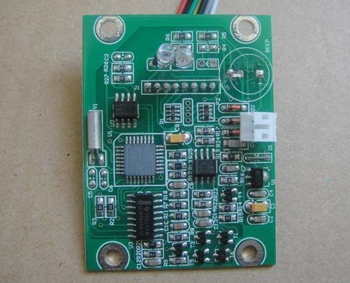
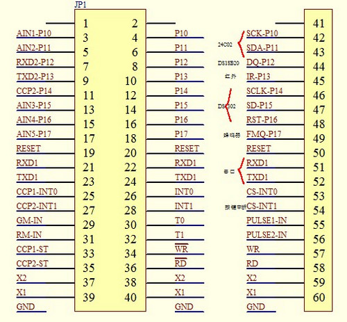
What are the smart lock chip models? What are the modules of the smart lock chip? In the smart lock architecture, the chip is the most important part of the smart lock's brain. There are still barriers to this technology in China. For users who want to understand the principle of smart lock chip, it is necessary to have a comprehensive understanding of the chip, mainly to provide the introduction of AT89S52 and AT24C02, carefully read this article, I believe there will be some conceptual knowledge.

The chip plays a role in controlling the operation of the smart lock. It is a key technology in the smart lock and controls the normal operation of the smart lock.
Chip technology is a common barrier faced by all IT industries in China. This technology has always been controlled and monopolized by the United States. At present, China has successfully developed a DSP fingerprint lock professional processing chip, the chip is generally packaged in Taiwan, domestic manufacturers burn the algorithm software; the vast majority of fingerprint lock manufacturers use domestic fingerprint algorithm chip.

The AT89S52 microcontroller is a low-power, high-performance CMOS 8-bit microcontroller. The chip contains 8K Bytes ISP (In-system programmable) flash-erase read-only program memory that can be rewritten 1000 times. The device uses ATMEL's high-density, non- Volatile memory technology manufacturing, compatible with the standard MCS-51 instruction system and 80C51 pin structure, integrates a general-purpose 8-bit central processor and ISP Flash memory unit in the chip, AT89S52 powerful microcomputer can be a lot of embedded control applications The system provides a cost-effective solution.
The AT89S52 has the following standard features: 8k bytes of Flash, 256 bytes of RAM, 32-bit I/O lines, watchdog timer, 2 data pointers, three 16-bit timers/counters, and a 6 vector 2 interrupt Structure, full duplex serial port, on-chip crystal oscillator and clock circuit. In addition, AT89S52 can be reduced to 0Hz static logic operation and supports two software selectable power saving modes. In idle mode, the CPU stops working and allows RAM, timers/counters, serial ports, and interrupts to continue working. In the power down protection mode, the RAM content is saved, the oscillator is frozen, and all work of the microcontroller stops until the next interrupt or hardware reset.
Smart Lock IC AT89S52 Pin Diagram
P0 port is an 8-bit open-drain bidirectional I/O port that can sink 8TTL gate current per pin. When pin 1 of P1 is written for the first time, it is defined as a high-impedance input. P0 can be used for external program data memory. It can be defined as the eighth bit of data/address.
P1 port is an 8-bit bidirectional I/O port with internal pull-up resistor. P1 buffer can receive 4 TTL gate current. After P1 port pin is written to 1, it is internally pulled high and can be used as input. P1 port is by external
When pulled down to low level, the output current will be due to the internal pull-up.
P2 port is an 8-bit bidirectional I/O port with an internal pull-up resistor. P2 port buffer can receive and output 4 TTL gate currents. When P2 port is written “1â€, its pin is pulled by internal pull-up resistor. High, and as input. Therefore, as an input, the pin of port P2 is pulled low externally and will output current. This is due to the internal pull-up. When the P2 port is used for accessing an external program memory or a 16-bit address external data memory, the P2 port outputs the upper eight bits of the address. When the address "1" is given, it uses the internal pull-up advantage. When reading and writing to the external eight-bit address data memory, the P2 port outputs the contents of its special function register.
P3 port is used as an optional function of some special functions of AT89S52. P3.0 RXD (serial input) P3.1 TXD (serial output) P3.2 / INT0 (external interrupt 0) P3.3 / INT1 ( External Interrupts 1) P3.4 T0 (Timer 0 External Input) P3.5 T1 (Timer 1 External Input) P3.6/WR (External Data Memory Write Strobe) P3.7/RD (External Data Memory) Read strobe)
Intelligent lock chip memory chip AT24C02 model detailsAT24C02 is a low-power CMOS type E2PROM from Atmel Corporation of the United States. It contains a 256×8-bit memory space, and has a wide operating voltage (2.5 to 5.5 V), a large number of erases (greater than 10,000), and a fast write speed (less than 10 Ms), anti-interference ability, data is not easy to lose, small size and other characteristics. Moreover, he is an I2C bus-based serial device for data read and write, occupies few resources and I/O lines, and supports on-line programming for real-time data access is very convenient. The on-chip address register included in the AT24C02. After every write or read of a data byte, the address register is automatically incremented to allow reading and writing to the next memory location. All bytes are read in a single operation.
To reduce the total write time, up to 8 bytes of data can be written in one operation. The I2C bus is a two-wire bus used for connection between IC devices. He transmits information between devices connected to the bus through two lines, SDA (serial data line) and SCL (serial clock line), and identifies each device according to the address. The AT24C02 uses the I2C protocol and uses master/slave bidirectional communication. Both the host (usually a microcontroller) and the slave (AT24C02) can work in the receiver and transmitter states. The master generates a serial clock signal (via the SCL pin) and issues a control word, which controls the direction of the bus transfer and generates start and stop conditions. Whether it is a master or a slave, an acknowledge signal ACK must be sent after receiving a byte. The AT24C02 control word consists of 8-bit binary numbers. After the start signal is issued, the host computer will issue a control word to select the slave and control the direction of the bus transfer.
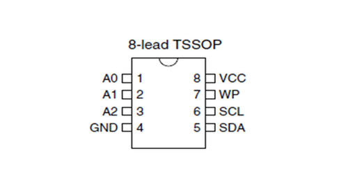
Smart lock chip memory chip AT24C02 pin diagram 
Pin description: SCL is serial clock:
The serial clock input pin is used to generate the clock for all device data transmission or reception. This is an input pin.
SDL is Serial Data/Address:
The bidirectional serial data/address pins are used to transmit or receive all data from the device. The SDL is an open-drain output pin that can be wired to other open-drain or open-collector outputs. A0, A1, A2 are Device Address Inputs:
When 24C02 is used, a maximum of 8 devices can be cascaded. If only one 24C02 is addressed by the bus, these three address input pins A0, A1, A2 can be left floating or connected to Vss. WP write protection:
If the contents of the WP pin connected to Vcc are all write-protected, they can only be read when WP, pin is connected to Vss or left floating, allowing the device to perform normal read/write operations.
Wittur Selcom Elevator Door Parts
Wittur Elevator Door Parts, Selcom Elevator Door Parts, Selcom Lift Door Parts, Wittur Lift Door Parts
Since 1977 Wittur supplies the lift industry with versatile and high-quality doors. Design flexibility, coupled with full range of certifications, makes Wittur landing doors suitable for every application. A wide variety of available finishings and executions allows them to fit in every environment: from residential to exclusive office buildings, from exterior installations to luxurious marine projects, from industrial buildings to hospitals.
Hydra Plus car door Hydra Plus is a door system which can be used with any kind of application from residential buildings up to highly frequented office buildings and hotels.
AUGUSTA ECO door is a new type of car door for residential and affordable housing elevator application.
Wittur Elevator Door Parts, Selcom Elevator Door Parts, Selcom Lift Door Parts, Wittur Lift Door Parts
CEP Elevator Products ( China ) Co., Ltd. , https://www.zjsmartcommercialescalators.com